



Every high-speed signal traveling through an AI server’s circuit board loses some energy to the board material itself. At the internet speed modern AI clusters now demand, that loss has become a meaningful engineering constraint.
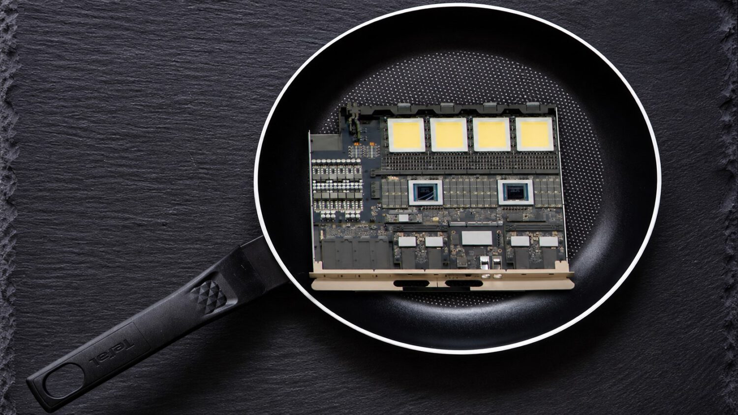
Industry sources, as reported by WCCFTech, say NVIDIA is evaluating polytetrafluoroethylene (PTFE), the compound behind the Teflon brand, for use in a future Rubin Ultra NVLink switch board or next-generation orthogonal mid-plane (the structural board connecting server modules). This is not a confirmed NVIDIA product announcement; the evaluation reportedly surfaced through industry activity connected to the OCP Summit and the TPCA Show.
What Dielectric Loss Actually Means
PTFE’s electrical appeal is straightforward: less of a signal’s energy dissipates before reaching its destination.
When a high-frequency signal travels through a PCB substrate, the material absorbs a portion of that signal’s energy as heat. A lower-loss material leaves more of the signal intact at the destination.
Industry commentary cited in the report suggests that even advanced M9-class laminates may not meet the most demanding projected channel-loss targets for boards exceeding 70 layers. By that analysis, PTFE is not a novelty but a logical next step on the low-loss laminate roadmap, though that characterization reflects industry inference rather than a confirmed NVIDIA position.
Why PCB Material, and Why Now
PCB-material improvement is presented in the report as a more immediately accessible engineering path than co-packaged optics, though that framing is analytical rather than a stated NVIDIA position.
NVLink switch boards are particularly sensitive territory. They carry dense, high-speed connections across multilayer layouts where signal budget margins are thin.
The Non-Stick Problem
The chemical property that makes PTFE electrically attractive also makes it one of the harder materials to build with in a multilayer board.
PTFE bonds poorly with other materials, complicating the lamination process central to building multilayer PCBs. Its low surface energy and chemical inertness create adhesion challenges, though specialized surface treatments can improve bonding to some degree.
PTFE is also comparatively soft and prone to dimensional instability. That creates real difficulties in drilling, copper plating, and lamination control.
Industry estimates, reported via WCCFTech and unverified by any manufacturer or NVIDIA disclosure, reportedly put current PTFE sample yields below 5%. One unnamed industry figure, cited in the report, questioned why PTFE had not been widely adopted in multilayer boards over the past 30 years. The manufacturing challenges listed above offer a reasonable part of that answer.
The Realistic Engineering Path
Available industry commentary points toward hybrid construction rather than a board built entirely from PTFE.
In that approach, PTFE would be deployed selectively in the highest-speed signal layers, while M10-class or structurally comparable materials would handle the remaining layers for yield, mechanical integrity, and cost. That would make PTFE an incremental component of the PCB stack-up, not a wholesale replacement for conventional copper-clad laminate.
What the Supply Chain Is Already Doing
Equipment investment among suppliers suggests preparation for evaluation and sampling, not confirmed production commitments.
Several PCB and materials suppliers reportedly tied to NVIDIA are acquiring equipment capable of processing PTFE. Vendors span China, Taiwan, and the United States, according to WCCFTech’s reporting of industry activity, though no transaction records or primary disclosures were available to confirm those supplier relationships.
An analyst cited in the report estimates the processing bottleneck could be resolved within roughly two years. Any commercial outcome, by the same forecast, would likely not emerge before 2028 to 2030. Both figures are projections, not schedules.
The Broader Signal
The pressure on PCB materials illustrates how quickly AI compute demands are cascading through the hardware supply chain, from silicon to switches to the boards carrying signals between them.
Whether PTFE closes the yield gap fast enough to matter depends on manufacturers solving long-standing processing challenges around bonding, drilling, plating, and high-volume dimensional control. If those problems yield to sustained engineering effort, a material best known for coating cookware could become a quiet but consequential part of the next generation of AI infrastructure. If they do not, PTFE is likely to remain a specialized option while the industry looks elsewhere for headroom.