



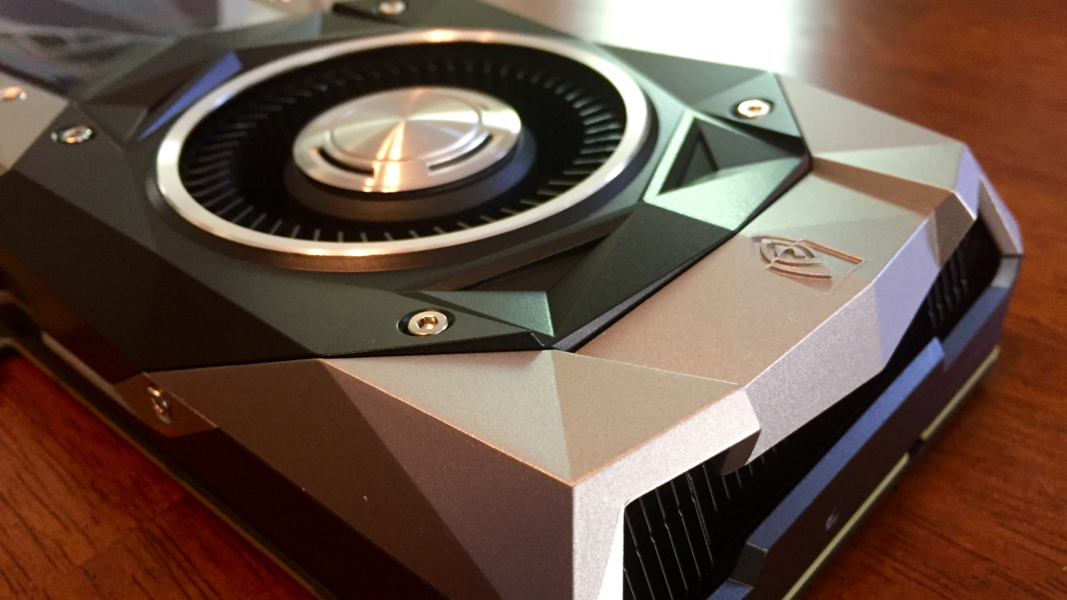
According to secondary reporting, a researcher transformed a $2,500 CMP-170HX mining card into a configuration sharing several hardware characteristics of an A100 that retails for roughly $20,000. Both cards share NVIDIA’s GA100 silicon family, and NVIDIA shipped the mining card with memory, compute, and interface capabilities locked at the factory.
A software tool called CMPunlocker had already attempted to expose some of that dormant hardware through graphics driver-level techniques. Results varied across project versions and revisions: VRAM capacity, shader modules, and PCIe bandwidth remained constrained in some configurations, and the project documentation describes NVLink and ECC support as experimental rather than guaranteed.
The Hardware Attack
The newer method goes beyond software by targeting the GPU’s fuse controller directly through carefully timed voltage disturbances.
A custom circuit built around an STM32G4 microcontroller reportedly intercepts PWMVID control signals running between the GPU and its voltage regulator. That circuit then generates precisely timed supply-voltage disturbances during fuse-controller activity. The objective is to push the fuse controller into a state where its security checks permit writes. That shift permanently alters the fuse settings governing memory, shader, and interface availability, according to the secondary reporting.
Reported Results
Nine of ten tested cards reportedly reached the full 80GB HBM2e configuration, with one falling short due to what appeared to be defective memory.
The successfully modified cards reportedly activated between 120 and 126 streaming multiprocessors, compared with 108 SMs on the standard A100 configuration the researcher cited. Reported FP16 throughput reached approximately 85.9 TFLOP/s against roughly 72.5 TFLOP/s for the retail A100 reference tested. These figures come from secondary reporting and have not been independently verified; the benchmark tool, precision mode, clock settings, and cooling conditions are not confirmed in the available evidence.
Why 80GB Matters for AI
For local AI inference, memory capacity is often a tighter constraint than raw compute throughput.
At 80GB of VRAM, a single card may reduce or avoid offloading for some workloads, allowing larger language models, longer context windows, and bigger batches. Raw compute throughput is a secondary consideration when model size is the binding limit. Readers exploring AI inference applications may find that capacity gains like these translate directly into more capable local deployments.
Security Significance
The demonstration suggests that hardware segmentation enforced through configurable fuse controls can be vulnerable to physical fault-injection techniques.
This finding does not mean all disabled GPU features are recoverable, nor that software locks are the only mechanism separating product tiers. It does indicate those controls warrant closer scrutiny than they typically receive.
Practical Limits and Risks
The process is demanding, time-consuming, and carries a real risk of permanent hardware damage.
Glitching time per card reportedly ranged from one to 48 hours, reflecting significant variability. The procedure requires board-level wiring, custom electronics, careful timing work, and repeated power cycling. A failed or incomplete attempt may void the warranty and can leave the card unstable, unusable, or without NVIDIA support or firmware coverage. Those facing instability after such attempts may benefit from reviewing common computer problems and their solutions.
What Remains Unverified
A single FP16 result does not establish full A100 equivalence across the workloads and conditions that matter most.
Sustained workloads, thermal behavior, ECC operation, and NVLink functionality are not demonstrated at scale in the available evidence. Power consumption and compatibility across different CMP-170HX hardware revisions are equally unverified. Independent replication is the next meaningful threshold this research needs to clear.